Seminar khoa học chủ đề: The materials for technologies at nano sizes
Vào 14h00, ngày 21/01/2026 Viện IAST tổ chức buổi trao đổi học thuật tại phòng họp lầu 5 Thư viện (cơ sở Tân Hưng) với nội dung chi tiết như sau:
1. GS. James Jebaseelan Samuel báo cáo về chủ đề: Ferrite based Nanocomposites for energy harvestor
Abstract: The demand for electric energy is vital for technological growth. Use of conventional batteries possess limited capacity for retention and require to be charged or replaced on a regular basis. Promoting the harnessing of biomechanical energy enables sustained energy production for as extended as the human body continues to be in activity. In this paper the Composite Piezoelectric Energy Harvester (CPEH) is proposed to scavenge the energy from the human motion. The flexible co polymer material of (Poly (Vinylidene Flouride-trifluoroethylene)) (P(VDF-TrFE)) is chosen as the piezoelectric material. The harvesting efficiency of the preferred piezoelectric material is enhanced by the nanoparticle additives. The ferrite-based nanoparticle such as Nickel Ferrite (NiFe 2 O 4 ) and Copper ferrite (CuFe 2 O 4 ) are synthesized and filled with bare (P(VDF-TrFE)). The Composite Piezoelectric Film (CPF) is achieved by the doctor blade coating method. The properties of the film which is fabricated is analysed using different characterisation techniques such as XRD, FTIR, AFM, Impedance analyser and DC probe station. The CuFe2O4 nanoparticle additives with (P(VDF-TrFE)) enhanced the harvested voltage of 7.7 V over the other.
2/ GS. Mikhail R. Baklanov báo cáo về chủ đề: Materials and Process Challenges in Interconnect Scaling in sub 10 nm technology nodes
Abstract: Traditional integrated circuits (ICs) utilized Al and SiO₂ as interconnect materials. However, with the advent of the 130–90 nm technology node (late 1990s), interconnect delay became a significant factor in signal propagation. To address this challenge, the industry transitioned from Al to Cu conductors and adopted low-κ dielectric materials. This shift aimed to reduce wire resistance and parasitic capacitance, thereby lowering RC delay and enhancing power efficiency. However, RC delay remains a key bottleneck; in 7–10 nm interconnects, it can exceed the intrinsic FET delay by a factor of 1,000 [1]. This is primarily due to increased copper resistivity at smaller dimensions (< 20 nm) and the degradation of ultralow-κ (ULK) dielectric properties during plasma-based processing in the damascene integration process.
One potential solution is to replace copper with alternative metals or alloys that exhibit lower resistivity at nanoscale dimensions, higher resistance to electromigration, and compatibility with barrier-less integration [2]. These materials enable the use of low-κ dielectrics with relatively higher intrinsic dielectric constants (κ ≈ 3.0) and enhanced mechanical properties (E > 10 GPa). The improved mechanical stiffness of such dielectrics facilitates the implementation of air gaps at specific interconnect levels, further reducing parasitic capacitance. This approach currently represents the leading strategy in the semiconductor industry.
However, as outlined in the International Roadmap for Devices and Systems (IRDS), upcoming technology nodes will demand further reductions in the effective dielectric constant (κ < 2.5 starting from 2030). One promising strategy to harness the benefits of these materials involves achieving damage-free integration of ULK materials by minimizing or eliminating plasma exposure. This can be accomplished through a transition from the damascene process to a subtractive etch approach, where the metal is first patterned, and subsequent trenches are filled with a flowable dielectric. Subtractive processing has been shown to maintain the initial κ-value of low-κ dielectrics post-integration [4]. Additionally, various metals with low line-width-dependent resistivity and good plasma etchability – such as ruthenium (Ru), molybdenum (Mo), and iridium (Ir) – are being explored as promising candidates for next-generation interconnects. A more robust integration method, known as semi-damascene, has recently been developed and reported by IMEC. In this technique, a Ru layer is patterned using plasma etching, resulting in an interconnect structure that incorporates air gaps to reduce parasitic capacitance [5].
1. G. Yeap, Proc. of the 2013 IEEE International Electron Devices Meeting (IEDM), 2013, 1.
2. J.-P. Soulié et al., J. Appl. Phys., 136, p. 171101, 2024.
3. L. Zhang et al., Appl. Phys. Lett., 107, p. 092901, 2015.
5. P. Singer. https://www.semiconductor-
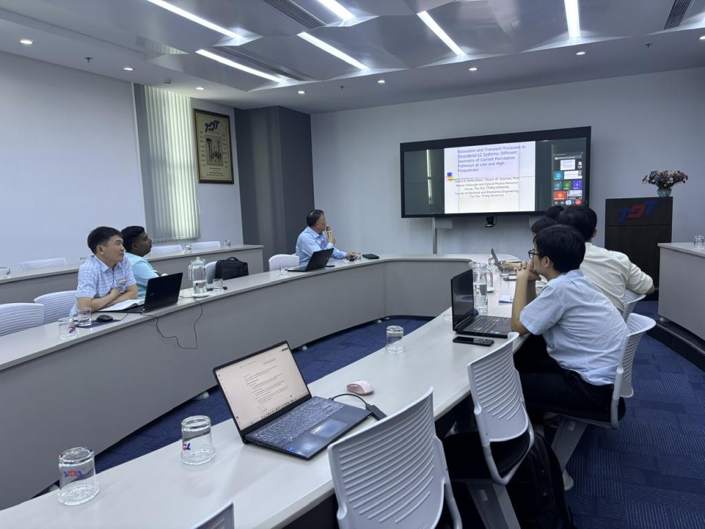
3/ PGS.TS Arkhincheev Valerii báo cáo về chủ đề: Relaxation and Transient Processes in Disordered LC Systems: Different Geometry of Current Percolation Pathways at Low and High Frequencies.
Abstract: This work studies relaxation processes and transient currents in a disordered multi-component LC system, consisting of inductive and capacitive reactances (non-dissipative elements). Usually at these LC systems the oscillations are possible and at first glance, relaxation processes seem impossible in non-dissipative systems such as LC systems. Nevertheless, at the percolation threshold, we establish that the relaxation and transient currents arise in this problem. The relaxation times for these processes are established for both low and high frequencies. It is interesting that the geometry of current percolation pathways are different at low and high frequencies. This surprising result obtained due to the exact solution for the multi-component system, consisting of two different types of inductors and two different capacitors with random displacement and connections. It was shown that the effective conductivity of such a non-dissipative disordered system has a real value. This means that effective dissipation arise in this non-dissipative system as result of excitation of the oscillations.
- Log in to post comments